


Support: GPIO Theory of Operation

This document applies to all TAMS GPIO interfaces. Data Lines The data lines of the TAMS GPIO interface consist of the lines designated for data input, DI0 through DI15, and those for data output, DO0 through DO15. Like all the TAMS GPIO lines, the default logic sense (polarity) of the data lines is low true. However, you can change the polarity of either set of data lines to high true with the TAMS GPIO card polarity in SICL configuration or in your SICL software. E.g. SICL C call igpioctrl (id, I_GPIO_POLARITY,<val>). You can configure the TAMS GPIO card data lines in either of the following two ways:
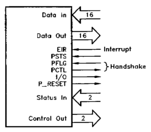
Note When using bi-directional mode, make sure the peripheral controlled by the TAMS GPIO card is bi-di compatible. If bi-di mode is selected and the peripheral is not bi-di compatible the TAMS GPIO card or peripheral's output buffers may be damaged. Given the two different configurations that are possible, this section discusses the data lines for the TAMS GPIO card with regard to each particular configuration you can use. The first subsection explains how the data lines function in Compatibility Mode, and the second explains how they function in Enhanced Mode. The final subsection then describes the choices available for data-in-clocking. Compatibility Mode When configured in Compatibility Mode, all the lines of the TAMS GPIO card appear the same as the HP 98622 GPIO interface. This is summarized in the following figure. Overview of Compatibility ModeThus, in Compatibility Mode, data input and data output are handled on separate, independent ports. Each port (the data input port and the data output port) has 16 lines (labeled 0 through 15) for a maximum of 16 bits each. You can configure the logic level of either port as either high-true or low-true. If you are using a TAMS GPIO card with the same peripheral device and same cable as an existing HP 98622 application, you should use Compatibility Mode. If your existing HP 98622 application uses an 8 bit data width, note that the upper data byte is undefined on the TAMS GPIO card. Although every effort was made to provide complete compatibility, there is no guarantee that the undefined lines on the TAMS GPIO card and the undefined lines on the HP 98622 will assume matching states at all times. This, however, will not represent any incompatibility or other problems. If both the GPIO interface and the peripheral device use the same 8-bit width, the other 8 bits cannot be controlled or examined by either the TAMS GPIO card or peripheral device. This assures that the state of the other 8 bits have no effect at all. In a properly designed application the GPIO interface and the peripheral device will always be configured with the same data widths. The next subsections describe the data input and the data output lines Compatibility Mode.
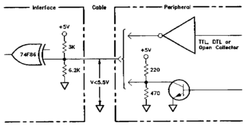
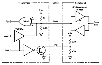
Data Input LinesIn Compatibiliy Mode, there are 16 data input lines labeled DI0 through DI15. Input lines DI0 through DI7 are the low (least-significant) byte, and DI8 through DI15 are the high (most-significant) byte. Three choices of data-in clocking are available for each byte or for the 16 bit word. Refer to the "Data-In Clocking" subsection later in this section for more information. The data input lines are TTL lines. A resistive divider biases open lines to approximately +3.4 volts. The following figure shows one data input line and some possible ways a peripheral device might connect to it. Caution The voltage applied to a data input line must never exceed + 5.5 volts. Electrical Detail of Data Input LinesThe following is a list of requirements for the data input lines. Any peripheral driver circuit must be compatible with these input requirements: Iinlow max = -2.3 ma (Vinlow = 0.4 V) Vinmax = 5.5 V Vinhigh > 2 V Vinlow < 0.7 V
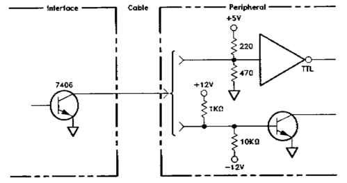
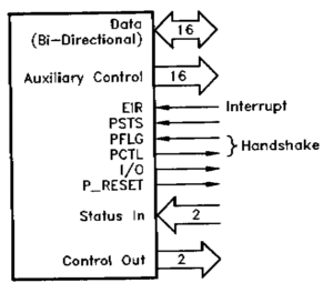
Data Output LinesIn Compatibility Mode, there are 16 data output lines labeled DO0 through DO15. Output lines DO0 through DO7 are the low (least-significant) byte, and DO8 through DO15 are the high (most-significant) byte. The data output lines are open-collector drivers which can sink a maximum current of 40 ma. For best flexibility, no internal pull-ups are used. Thus, the peripheral device must provide a pull-up to a positive voltage, not to exceed 30 volts. The following figure shows one data output line and some possible ways a peripheral device might connect to it. CAUTION Do not apply a negative voltage to the data output lines. Electrical Detail of Data Output LinesThe following is a list of requirements for the data output lines. Any peripheral receiver circuit must be compatible with these output requirements: VoutLow (IoutLow = 16 ma) = 0.4 V max (IoutLow = 40 ma) = 0.7 V max VoutHigh (open collector) = 30 V max Ioutlow = 40 ma max Iouthigh(Vout = 30 V) = 250 ua Enhanced Mode When configured in Enhanced Mode, the TAMS GPIO card uses a bi-directional data port on the lines normally designated for data input (DI0 through DI15). The data output lines (DO0 through DO15) are thus free to be used as independent auxiliary control lines. This is summarized in the following figure: Overview of Enhanced ModeEnhanced Mode allows more interfacing flexibility than Compatibility Mode. However, Enhanced Mode is only appropriate for use with peripheral devices that have bi-directional data ports. The next subsections describe the bi-directional data lines and the auxiliary control lines in Enhanced Mode.
Bi-Directional Data LinesIn Enhanced Mode, the bi-directional data port is TTL level. It has resistive pull-ups up to + 5 volts. The peripheral device must use a data port compatible with bi-directional protocol. The TAMS GPIO card port direction is controlled by the I/O (Input/Output) direction control line. Likewise, the peripheral device must use the I/O line to set the proper direction of its data port. The I/O line is low when the TAMS GPIO card drivers are enabled (output) and is high when the TAMS GPIO card drivers are disabled (input). The following figure shows one bi-directional data line and one way a peripheral device might connect to it. Caution The voltage applied to the bi-directional data lines (DI0 through DI15) must never exceed + 5.5 volts. Electrical Detail of Bi-Directional Data Lines Caution When connected to a TAMS GPIO card in Enhanced Mode, the peripheral device must never attempt to drive the data lines at the same time that the TAMS GPIO card drivers are enabled. Also, the peripheral device must not exceed TTL voltage or current levels on the data lines. Failure to follow these specifications can result in damage to the TAMS GPIO card hardware interface or peripheral device. If your peripheral device cannot conform to these specifications, do not use Enhanced Mode. See the previous subsection on "Compatibility Mode" instead.
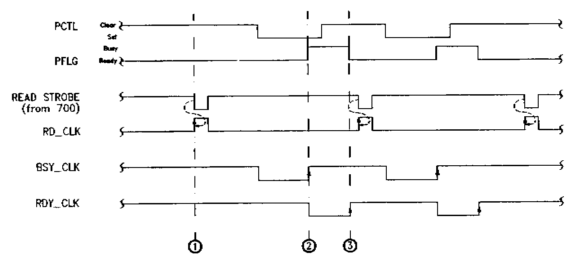
Auxiliary Control LinesThe auxiliary control lines created by Enhanced Mode are connected to the 7406 open-collector drivers described in the previous "Compatibility Mode" subsection. They have the same 30 volt, 40 ma limits. Like the control output lines (CTL0 and CTL1), the auxiliary control lines are write-only and use no handshake with the peripheral device. NOTE The auxiliary control lines created by Enhanced Mode inherit the same logical polarity configured for the data output port. Programming Notes. In C programs, the auxiliary control lines are set by the I_GPI0_AUX parameter of the igpioctrl function in HP SICL. For example: igpioctrl (id , I _ GPI 0 _AUX , value); For more information, please refer to the HP SICL documentation. In HP BASIC/UX 700 programs, the auxiliary control lines are set by CONTROL register 4. For more information, please refer to the HP BASIC/UX 700 documentation. Data-In Clocking Three choices of data-in clocking are available for each byte or for the 16-bit word. You set this in the TAMS GPIO card read_clk or Read Clock configuration value in your software. As explained earlier, the 16 data input lines are divided into two data bytes. The lower, least-significant byte consists of data input lines DI0 through DI7. The upper, most-significant byte consists of data input lines DI8 through DI15. Data-in clocking can be selected from any of three clock sources for both upper and lower bytes. The following figure shows the timing diagram for data-in clocks on a full standard read. The clocking for the other operating modes, including pulse mode, follows these same guidelines. Data-In Clocking Timing Diagram The next subsections describe the three clocks which can be selected to latch data. The descriptions are applicable to either the upper or lower byte.
Read ClockThe Read clock causes the data to be latched into the data input register when the register is read. (See the previous figure, phase 1.) The Read clock accomplishes this by clocking the register on the leading edge of the read strobe of the register. During a DMA transfer, the Read clock causes the data to be latched with DMA acknowledge which is generated by the DMA controller.
Bsy ClockThe Busy clock latches the data into the data input register by the leading edge of the PFLG line. (Refer to the previous figure, phase 2.) This transition also clears the PCTL line. This is the ready-to-busy transition of the PFLG line.
Rdy ClockThe Ready clock latches the data into the data input register by the trailing edge of the PFLG line. (Refer to the previous figure, phase 3.) This is the busy-to-ready transition of the PFLG line.
Peripheral Information LinesTen lines control the exchange of information between the TAMS GPIO card GPIO interface and the peripheral device. Five of these lines are outbound to control the peripheral:
The other five peripheral information lines are inbound to communicate the state of the peripheral:
All 5 incoming lines have Schmitt trigger receiver circuits. These circuits accept signals with slow rise and fall times. They also provide good noise immunity. Although the voltage on these lines must not exceed 5.5 volts, there are no restrictions on the input rise and fall times. All of the peripheral information lines are described in the following subsections.
Peripheral Control and Peripheral Flag Handshake Lines (PCTL and PFLG)The peripheral control line (PCTL) and the peripheral flag line (PFLG) are used as a 2-wire handshake between the TAMS GPIO card interface and the peripheral device. The TAMS GPIO card interface controls the PCTL line, and the peripheral device controls the PFLG line. The TAMS GPIO card provides both handshake modes of the HP 98622, plus an additional async output mode. Also, the logic sense of the PCTL and PFLG lines on the TAMS GPIO card can be configured differently. Like all the TAMS GPIO card lines, PCTL and PFLG have the default logic sense (polarity) of low-true. The polarity of either or both the PCTL and PFLG lines can be changed with the TAMS GPIO card polarity configuration value in your software. If you are porting an HP 98622 application, notice that the bits in the polarity field correspond to DIP switches on the HP 98622 interface card. However, many old cards had " 1" and "0" markings that were backwards from the electrical state of the switch. When transferring your old settings to the polarity value, keep in mind that all the bits might be upside-down (0® 1). The following subsections describe each handshake line (PCTL and PFLG), as well as the handshake modes for the TAMS GPIO card.
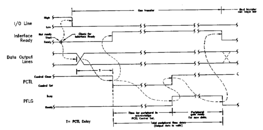
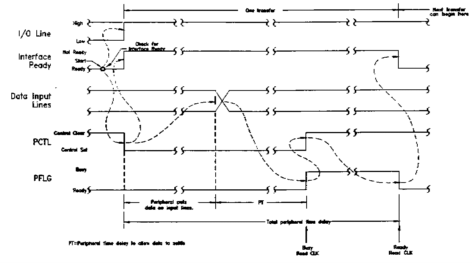
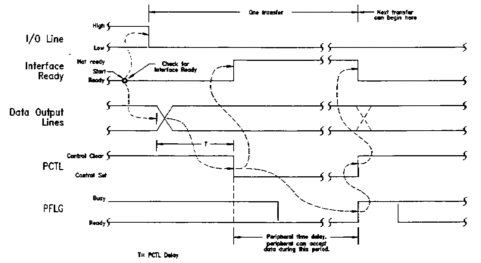
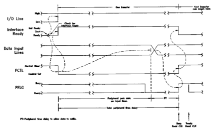
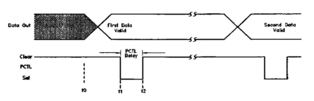
PCTL LineThe PCTL line is an outgoing line to the peripheral. PCTL has two states: set and clear. The TAMS GPIO card sets the PCTL line to start a handshake. The peripheral device clears the PCTL line when a ready-to-busy transition occurs on the PFLG line. (A ready-to-busy transition is when PFLG goes from the ready state to a busy state.) During an output transfer, PCTL is delayed to allow new output data to settle. This delay is explained in the next subsection, "PCTL Delay." PCTL Delay. You can select the delay (settling time) from when data is placed on the GPIO bus to when PCTL is Set during an output data transfer. The delay selection is set with the TAMS GPIO card configuration (SICL ioconfig) or it can be changed from within the software with igpioctrl (id,I_GPIO_PCTL_DELAY, <val>). Accepted values are HP 2074/5 compatible. In addition, a direct value in nanoseconds could be specified. Acceptable values in nanoseconds are between 90 and 245,000 inclusive (90 nanoseconds to 245 microseconds). The delay selections are: 200 ns, 400 ns, 700 ns, 1.2µs, 2 µs, 5 µs, 10 µs, and 50 µs. PFLG Line. The PFLG line is an incoming line from the peripheral device. PFLG must be driven to complete a data transfer. PFLG has two states: ready and busy. When the peripheral device is ready to transfer data, it responds by setting PFLG to ready. When the computer sets PCTL, the computer has initiated a data transfer either in or out, depending on the state of the I/O line. (See the "Input/Output Direction Control Line (I/O)" later in this section.) After the data transfer occurs, the peripheral device responds by setting PFLG to busy. This causes the TAMS GPIO card to clear the PCTL line on the ready-to-busy transition. In the full handshake mode, the interface waits until the peripheral device makes PFLG ready before initiating another data transfer. In the pulse handshake mode, the interface initiates the transfer without waiting. Refer to the next subsection on "Handshake Modes" for more information. Handshake Modes. Like the HP 98622, the PCTL and PFLG lines on the TAMS GPIO card can be used for full-mode or pulse-mode handshakes. Additionally, the TAMS GPIO card provides an async-mode for output. You set the handshake modes with the TAMS GPIO card mode or Handshake configuration value in your software. All of the handshake modes for the TAMS GPIO card are explained in the following subsections. Full-Mode Handshakes. With full-mode handshakes, the computer first checks to see that the peripheral device is Ready before initiating the transfer of each byte or word. With this handshake mode, the interface detects Ready when both PCTL is Clear and PFLG is Ready. If the peripheral device does not indicate Ready, the computer waits until a Ready is indicated. During a write cycle, when a Ready is sensed, the computer drives the I/O line Low, then places data on the appropriate data lines. The interface then waits the PCTL delay time before initiating the transfer by placing PCTL in the Set state. The peripheral acknowledges the computer's request by placing the PFLG line Busy; this PFLG transition automatically Clears the PCTL line. However, the computer cannot initiate further transfers until the peripheral is Ready with full-mode handshake. Ready is not sensed until both PCTL is Clear and PFLG is Ready. The data on the data lines is held valid from the time PCTL is Set until after the peripheral device indicates Ready. The peripheral may read the data any time within this time period. The following two figures show the order of events during full-mode output and input operations. Full Mode Timing Diagram:
Output Operation |